

Time:2023-06-25 Views:788
In electronic assembly, printed circuit boards are a key component. It is equipped with other electronic components and connected to the circuit to provide a stable working environment for the circuit. The general circuit configuration can be broadly divided into three categories:
【 Single panel 】 The metal circuit that provides part connections is arranged on an insulated substrate material, which is also a support carrier for installing parts.
【 Double sided board 】When a single sided circuit is not sufficient to provide electronic component connection requirements, the circuit can be arranged on both sides of the substrate and through hole circuits can be built on the board to connect the circuits on both sides of the board.
【 Multi layer board 】In complex application requirements, the circuit can be arranged into a multi-layer structure and pressed together, and through hole circuits can be built between layers to connect the circuits of each layer.
【PCB manufacturing process】
The production of PCBs is very complex. Taking four layer printed boards as an example, the production process mainly includes PCB layout, core board production, inner layer PCB layout transfer, core board drilling and inspection, lamination, drilling, copper chemical precipitation of hole walls, outer layer PCB layout transfer, outer layer PCB etching, and other steps.
【PCB layout】
The first step in PCB production is to organize and check the PCB layout. The PCB manufacturing factory receives CAD files from the PCB design company. As each CAD software has its own unique file format, the PCB factory will convert them to a unified format - Extended Gerber RS-274X or Gerber X2. Then the factory engineers will check whether the PCB layout conforms to the manufacturing process and whether there are any defects or other issues.
【Production of core board】
Clean the copper clad plate. If there is dust, it may cause the final circuit to short or open.
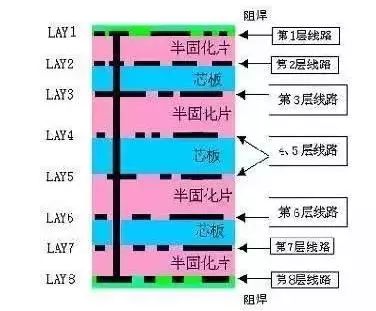
The following figure is the legend of an 8-layer PCB, which is actually composed of 3 copper clad boards (core boards) and 2 copper films, and then glued together with semi cured sheets. The production sequence starts from the middle core board (4, 5 layers of circuits), continuously stacking them together, and then fixing them. The production of a 4-layer PCB is also similar, except that only one core board and two copper films are used.
【Transfer of inner PCB layout】
First, we need to create a two-layer circuit for the middle core board. After cleaning the copper clad plate, a layer of photosensitive film will be covered on the surface. This film will solidify when exposed to light, forming a protective film on the copper foil of the copper clad plate.
Insert two layers of PCB layout film and double layer copper clad plate, and finally insert the upper layer of PCB layout film to ensure accurate stacking position of the upper and lower layers of PCB layout film.
The photosensitive machine uses a UV lamp to illuminate the photosensitive film on copper foil. Under the transparent film, the photosensitive film is cured, while under the opaque film, there is still no cured photosensitive film. The copper foil covered under the solidified photosensitive film is the required PCB layout circuit, equivalent to the function of laser printer ink for manual PCBs.
Then clean the uncured photosensitive film with alkaline solution, and the required copper foil circuit will be covered by the cured photosensitive film.
Then use strong alkali, such as NaOH, to etch off the unnecessary copper foil.
Tear off the cured photosensitive film and expose the required PCB layout copper foil.


+86 18825066881 (Mr. Liu)

sales@lhdxlb.com

For inquiries about our products or price list, please leave us and we will contact you within 24 hours.


